Senba Sensing초전기 적외선 감지에 초점19년 이상의 전문 제조 PIR 센서
![]()
Senba Sensing초전기 적외선 감지에 초점19년 이상의 전문 제조 PIR 센서
![]()

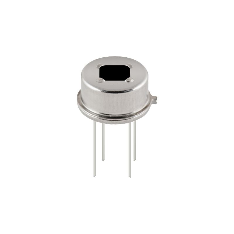
PROD Model:BS412
Window Size:3*4mm
Output Signal:High and low level output
Sensing Distance:12M(Lens SB-F-02) See lens selection for different distances
Sensing Angle:120°(horizontal direction)
Working Voltage: 2.2-3.7V
Static Power Consumption: <12uA
It is a low power pyroelectric
infrared sensor(PIR) for motion detection . Using the MCU for
communication,when the RS412 performs continuous motion sensing,the MCU
does not need to be activated, it only activates the external MCU when
motion is detected. Motion detection results are sent out via the output
interrupt signal.The algorithm for motion detection is programmable and
can be changed by external MCU configuration, The PIR signal is
converted into a 14-bit digital value on the chip, and then enters the
motion algorithm detection unit. All signal processing is digital and
supports motion detection result output and raw data output.
Power supply voltage range 1.6V-5.5V
Programmable detection standard and working mode
Digital signal processing
Ultral low power consumption
Power supply voltage measurement
Temperature measurement
Fast and stable power-on
1.Technical data
Description | Symbol | Min | Typical | Max | Unit | Remarks |
VDD voltage | VDD | -0.3 | 5.5 | V | 25℃ | |
Analog pin voltage | -0.3 | VDD+0.3 | V | 25℃ | ||
Digital pin voltage | -0.3 | VDD+0.3 | V | 25℃ | ||
Storage temperature | -30 | 80 | ℃ |
2.Operating Conditions ( TAMB = +25℃ Typical VDD=3V)
Description | Conditions | Symbol | Min | Typical | Max | Unit | ||||||
Operating temperature | ||||||||||||
Operating temperature range | -20 | +70 | ℃ | |||||||||
Operating Voltage | ||||||||||||
Supply voltage | VDD | 1.6 | 5.5 | V | ||||||||
Supply current | ||||||||||||
Supply current, VPIR regulator on | VDD=3V, no load | IDD1 | 6 | 8 | µA | |||||||
Supply current, VPIR regulator off | VDD=3V, no load | IDD | 3 | 5 | µA | |||||||
Input parameter SERIN | ||||||||||||
Input low voltage | VIL | 0.2 | VDD | |||||||||
Input high voltage | VIH | 0.8 | VDD | |||||||||
Input Current | VSS<VIN<VDD | IIN | -1 | 1 | µA | |||||||
Digital clock low time | tL | 200 | ns | |||||||||
Digital clock high time | tH | 200 | ns | |||||||||
Data Bit Write Time | tBW | 2/FCLK | 5/FCLK | µs | ||||||||
Write timeout | tWL | 16/FCLK | µs | |||||||||
Data input and output pins INT/DOCI | ||||||||||||
Input low voltage | VIL | 0.2 | VDD | |||||||||
Input high voltage | VIH | 0.8 | VDD | |||||||||
Output current high | VOL>(VDD-1V) | IOH | -200 | µA | ||||||||
Output current low | VOL<1V | IOL | 200 | µA | ||||||||
Input capacitance | 5 | pF | ||||||||||
Force read setup time | TFR | 2/FCLK | ||||||||||
Interrupt clear time | tCL | 2/FCLK | ||||||||||
Digital clock low time | tL | 200 | tRA | ns | ||||||||
Digital clock high time | tH | 200 | ns | |||||||||
Read timeout | tRA | 4/F | µs | |||||||||
Description | Conditions | Symbol | Min | Typical | Max | Unit
| ||||||
Supply voltage measurement | ||||||||||||
Resolution | 590 | 650 | 720 | µV/count | ||||||||
ADC output range | 2^13 | 2^14-511 | Counts | |||||||||
Temperature measurement (requires single point calibration) | ||||||||||||
Resolution | 80 | Counts/K | ||||||||||
ADC output range | 511 | 2^14-511 | Counts | |||||||||
Value at 300K | 6700 | 8200 | 9900 | Counts | ||||||||
Oscillator and Filter | ||||||||||||
Filter cutoff frequency | FCLK * 1.41 / 2048 / PI | Hz | ||||||||||
HPF cutoff frequency | FCLK /16 * 1.41 / 2048 / PI | Hz | ||||||||||
On-chip oscillator frequency | FOSC | 56 | 64 | 74 | kHz | |||||||
System clock | FCLK | FOSC/2 | ||||||||||